Testimonials
Services
General Guidelines on Interview tips
Resume Template
Mock Interview: Experienced
General Guidance call
Discovery Call for Semiconductor Proffesionals
LinkedIn Profile Optimization
About me
Frequently asked questions
Is VLSI a good career in India for the next 10 years?
Yes, especially for engineers who build strong fundamentals. India's semiconductor ecosystem is expanding with new fabs, ATMP facilities, and a rapidly growing number of design centres, which is pushing demand for skilled engineers in physical design, design, and verification. The entry barrier is real — companies expect solid digital electronics, CMOS, and timing concepts — but prepared candidates find stable, well-paying roles where salaries grow significantly with domain depth and experience.
What is the VLSI physical design engineer salary in India for freshers and experienced engineers?
It depends mainly on the company type and your hands-on depth. Fresher physical design roles at service-based companies typically start around ₹4–7 LPA, while product companies and semiconductor MNCs often pay more, particularly for candidates from strong M.Tech programmes. With 3–5 years of real flow experience in floorplanning, CTS, and timing closure, salaries commonly move into the ₹12–25 LPA range, and engineers with advanced-node, low-power, and STA expertise earn substantially higher. Tool proficiency and timing depth are the biggest salary levers.
How to become a VLSI physical design engineer in India as a fresher?
Build the stack in order: digital design and CMOS fundamentals, static timing analysis, then the physical design flow itself — floorplanning, placement, CTS, routing, and signoff checks like DRC/LVS. Since colleges rarely teach industry tools, add hands-on practice through a course or lab access, complete one small end-to-end project, and target service-based companies that hire freshers into PD. Getting your resume and preparation strategy reviewed by a working physical design engineer — for example, through a 1:1 mentoring call like those offered by VLSI_Growth — helps you avoid months of wasted effort at the shortlisting stage.
How to learn VLSI physical design from scratch?
Sequence matters more than speed. First master digital logic and CMOS basics, then static timing analysis (setup/hold, slack, timing paths), then each physical design stage in order — floorplanning, placement, clock tree synthesis, routing, and physical verification — focusing on why each step exists. After the theory layer, move to tool practice using whatever access you can arrange (academic tools, open-source flows, or a structured course), and finish with a mini project you can defend in interviews. Learning concepts without ever applying them to a real flow is the most common reason freshers stall.
Which VLSI physical design course is best for freshers in India?
Judge any course on four criteria: does it cover the full flow from floorplanning to signoff, does it include real or realistic tool practice, does it teach STA depth instead of just tool clicks, and do you finish with a project you can explain confidently. NPTEL works well as a low-cost theory foundation, while paid VLSI training institutes add lab exposure — the right pick depends on your background and budget. If you are confused between options, a short guidance session with a practising physical design engineer can tell you whether a course actually fits your profile before you spend money.
Is the VLSI physical design NPTEL course enough to get a job in physical design?
NPTEL gives you strong conceptual grounding — flow stages, algorithms, and timing basics — but on its own it is usually not enough, because companies also screen for tool exposure, project work, and interview clarity. Treat NPTEL as your theory layer, then add hands-on flow practice, at least one project you can explain in depth, and mock interview practice. Candidates who pair the course with demonstrated practical work consistently outperform those who rely on certificates alone.
Are there enough VLSI physical design jobs for freshers in India?
Yes, but through a specific entry route. Most fresher physical design hiring happens at service-based companies and design-service arms of MNCs, which train freshers on live flows, while product companies mostly hire experienced engineers or premium institute M.Tech graduates. So the practical path is: get in through a service company, build 2–3 years of flow experience, and then move to product roles. Overall VLSI openings are fewer than software openings, which means preparation quality — fundamentals, tools, projects, and interview practice — decides outcomes more than vacancy counts.
What does a realistic VLSI job roadmap for a fresher look like?
A practical VLSI job roadmap looks like this: solidify digital electronics, CMOS, and computer architecture basics; pick one domain early, because the VLSI career path for freshers differs sharply between RTL design, verification, and physical design; spend 3–4 focused months on that domain plus tool exposure; build one project or internship; then prepare a VLSI-focused resume, apply off-campus to service companies, seek referrals on LinkedIn, and rehearse mock interviews before the hiring season. Plan on 6–12 months of consistent preparation, and get the sequence reviewed by a mentor so you do not prepare in the wrong order.
What is a VLSI design engineer, and how is the role different from a physical design engineer?
A VLSI design engineer is a broad term for engineers working on chip design — most often front-end roles like RTL design (writing and synthesizing HDL) or sometimes verification. A physical design engineer is a backend specialist who converts the synthesized netlist into the actual chip layout — floorplanning, placement, clock tree synthesis, routing, and timing/DRC/LVS signoff. In Indian job postings, "VLSI design engineer" usually signals front-end work, while "physical design engineer" explicitly means backend. Front-end is more coding- and architecture-centric; physical design is more tool-flow and timing-centric, and both are well-paid long-term paths.
What is macro in VLSI physical design?
A macro is a pre-designed, pre-verified layout block — such as an SRAM memory, processor core, PLL, or third-party IP — that is instantiated as a fixed unit in the chip instead of being built from standard cells. Macro placement is one of the most critical floorplanning decisions, because poorly placed macros cause congestion, routing detours, and timing violations, which is why engineers align macro pins toward their logic, add halos/keepouts, and group related macros together. Hard macros versus soft macros and macro placement guidelines are among the most frequently asked physical design interview topics.
What is congestion in VLSI physical design, and how is it fixed?
Congestion occurs when the routing demand in a region exceeds the available routing tracks, so the router cannot connect all nets cleanly — it is reported as overflow after placement or global routing. Typical causes include high cell density in one area, macros blocking routing channels, too many pins concentrated in a small region, and excessive buffers. Fixes include reducing placement density, improving macro placement, enabling congestion-aware placement, spreading cells, and removing unnecessary buffers. Interviewers ask this often because solving congestion requires understanding how floorplanning, placement, and routing interact.
What is routing in VLSI physical design?
Routing is the stage where all placed cells and blocks are physically connected using metal layers according to the netlist, after clock tree synthesis. It happens in phases: global routing plans each net's path across routing regions, track assignment allocates actual tracks, and detailed routing creates the final wires and vias while obeying DRC rules. Because real wire parasitics (resistance and capacitance) change delays, the design goes through timing analysis again post-route. Expect interview questions on routing layers, vias, congestion handling, and why routing must follow CTS.
Which topics do physical design interview questions for freshers usually cover?
Expect a mix of fundamentals and flow knowledge: CMOS inverter behaviour, setup and hold checks, slack, timing paths, and a walkthrough of the physical design flow — floorplanning (utilization, macro placement), placement, CTS (why it is needed, skew), routing, and DRC/LVS. Interviewers also dig into your projects and often ask basic scripting (TCL/Python), since PD flows are script-driven. For fresher roles at service companies, clarity on STA concepts and the end-to-end flow matters more than tool experience, so practise explaining these out loud, ideally in a mock interview.
Is memorizing physical design interview questions and answers enough to crack an interview?
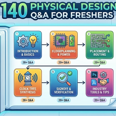
No — this is the most common reason candidates get rejected. Interviewers cross-question two or three levels deep ("why is CTS done before routing?", "what if setup fails after routing?"), and memorized answers collapse under follow-ups. Curated sets like the Physical Design 140 QnA are best used as a self-test: attempt each question, mark whatever you cannot explain confidently, and revisit the underlying concept. Combine that with your own project explanations and one or two mock interviews so you answer naturally instead of reciting.
What do physical design interview questions and answers for experienced engineers usually focus on?
At 3+ years, interviews shift from definitions to ownership: deep dives into projects you actually handled — congestion or timing closure problems you solved, hold violation fixes, trade-offs you chose, and results you delivered. Expect low-power techniques (multi-voltage domains, power gating, UPF basics), IR drop, ECO flows, crosstalk/SI, and debugging scenarios where the interviewer keeps asking "what else could it be?". Rehearse four or five detailed project stories with concrete numbers, and if you have not interviewed recently, an experienced-level mock interview helps you handle cross-questioning before the real one.