Testimonials
Services
College Student Session

Resume & Career Guidance Pack
Clarity and Reset Session
Conversations That Matter
From Resume to Role: Land the job you deserve
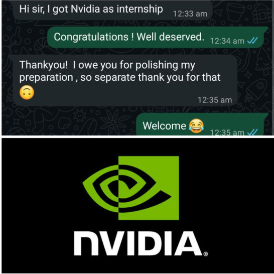
Interview Edge Package

Resume Review + Written Feedback & Re-check
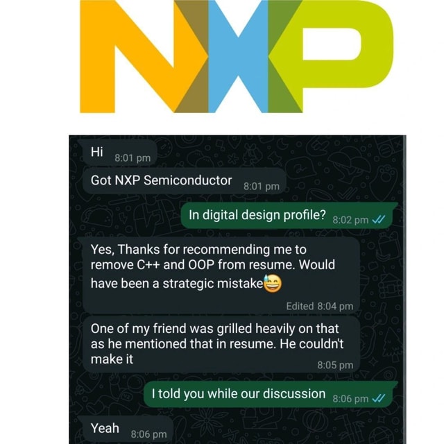
Navigating Office Politics & Power Dynamics
Priority DM : Quick Career Guidance !
About me
- Thanks to Rishabh for helping me handle office politics wisely. His guidance taught me to stay calm, think strategically, and respond with confidence instead of reacting emotionally.Recommended by Ramesh Shukla on

- I gained clients thanks to Rishabh’s guidance, as someone from a humanities background, I learned to apply creativity and logic practically, pitch my work confidently, and achieve real-life results.Recommended by Anonymous on
Frequently asked questions
What is VLSI design and technology engineering, and is it a good career option in India?
VLSI stands for Very Large Scale Integration, and VLSI design and technology is the branch of engineering that deals with designing and building integrated circuits — the silicon inside phones, cars, laptops, and data centres. Several Indian universities now offer dedicated B.Tech and M.Tech programmes in this field, and its popularity has grown because global semiconductor companies are steadily expanding their design centres in India. If you enjoy digital electronics, circuits, and logic, it is one of the most future-proof hardware careers available today, with roles in design, verification, physical design, and testing at companies like NVIDIA, AMD, Qualcomm, Synopsys, and Cadence.
What is a VLSI design engineer, and what does the role actually involve?
A VLSI design engineer builds the digital logic that goes into a chip. Depending on the team, the work can involve RTL design using Verilog or VHDL, functional verification using SystemVerilog and UVM, physical design, DFT, or post-silicon validation. Day to day, you write and debug hardware description code, run simulations, work with EDA tools, and collaborate closely with architecture and software teams. It is a detail-heavy role because a single bug discovered after fabrication is extremely expensive to fix.
How to become a VLSI design engineer in India?
The most common path is a B.E./B.Tech in ECE, EEE, or VLSI, followed by strong fundamentals in digital electronics, CMOS design, Verilog/SystemVerilog, and computer architecture. Many engineers also pursue an M.Tech in VLSI, since several product companies prefer MTech candidates for core design roles, though BTech candidates with strong projects and interview skills do get in. Focus on hands-on labs, mini-projects, and internships, because core semiconductor interviews test concepts deeply rather than marks alone. Getting guidance from someone already working in the industry early on saves a lot of guesswork about which skills matter for which role.
How to learn VLSI design from scratch as a complete beginner?
Start with digital logic design — number systems, combinational and sequential circuits — because everything in VLSI rests on it. Then learn a hardware description language like Verilog or VHDL and practise writing and simulating small modules using free or student versions of EDA tools. Once comfortable, move to understanding how to design a VLSI circuit end to end: study CMOS fundamentals, build small designs like counters, FSMs, and FIFOs, and then learn the VLSI design flow to see how all the stages fit together. A few months of consistent, hands-on practice usually puts you ahead of most peers.
What is the VLSI design flow, and why do interviewers ask about it so often?
The VLSI design flow is the step-by-step process of turning an idea into a working chip: specification and architecture, RTL design, functional verification, synthesis, static timing analysis, physical design (floorplanning, placement, clock tree synthesis, routing), sign-off checks, fabrication, and finally testing. Interviewers love this question because your answer instantly reveals whether you understand how the stages connect, where bugs get caught, and which stage you actually want to work in. If you can explain each block, its trade-offs, and the tools used at each step, you stand out in both fresher and experienced interviews.
Which VLSI design course is worth doing to get a job in the semiconductor industry?
Pick a VLSI design course that is heavy on hands-on work — it should cover digital design, Verilog/SystemVerilog, CMOS concepts, and give you real tool exposure plus projects you can defend in interviews. If you are open to full-time study, an M.Tech-level VLSI design and embedded systems course from a reputed institute like the IITs or NITs is well respected by recruiters, while working professionals often choose shorter industry-led programmes. Whatever you pick, check who is teaching, whether industry experience is involved, whether there is mock interview or placement support, and whether past students have actually landed core roles at companies like Qualcomm, Micron, or MediaTek.
What are the most common VLSI interview questions for freshers?
For freshers, interviewers usually start with digital logic design — muxes, flip-flops, counters, and setup/hold time basics — then move to Verilog coding questions like sequence detectors and FIFO depth calculation, followed by CMOS fundamentals such as transistor-level NAND/NOR diagrams and static timing analysis basics. Many companies also include aptitude, puzzles, and a deep discussion of your academic projects. The biggest mistake freshers make is memorising answers without being able to derive them — interviewers deliberately ask "why" follow-ups, so practise explaining every concept aloud and do a few mock interviews before the real thing.
What type of VLSI interview questions for experienced engineers should I expect?
At the experienced level, the interview revolves around your projects — expect deep, layered grilling on the architectures you have worked on, the bugs you have debugged, and the trade-offs you made and why. Alongside that, you will face advanced questions from your specialisation, whether that is design verification (UVM, assertions, functional coverage), RTL design, physical design, or DFT, plus scripting (Python, Perl, Shell) and system-level understanding. Senior rounds often test ownership and cross-team collaboration. The best preparation is restructuring your resume around measurable contributions and rehearsing your project stories, because experienced interviews are won on depth, not breadth.
Where can I find genuine VLSI interview questions and answers — and is a VLSI interview questions with answers PDF enough to prepare?
You will find plenty of VLSI interview questions and answers in standard textbooks, GitHub repositories, and interview-experience posts shared by candidates on job communities, and a VLSI interview questions with answers PDF is handy for quick revision in the final week. The catch is that PDF answers are often shallow, occasionally wrong, and rarely explain the reasoning interviewers probe for. Use them as a topic checklist, not as your main preparation — build concepts from fundamentals, practise articulating answers aloud, and get feedback through mock interviews, because that is what converts preparation into offers.
How do I find semiconductor jobs in India for freshers?
Start with on-campus placements wherever core companies visit, but do not stop there — most semiconductor design centres in India also hire freshers through off-campus drives, company career pages, and LinkedIn referrals from employees. Semiconductor jobs in India for freshers are concentrated in roles like design, verification, physical design, and DFT, so your resume should clearly show relevant projects and fundamentals, because core companies shortlist heavily on skills. Internships are another strong entry route, and many convert into pre-placement offers. If you are not from a tier-1 college, a referral combined with strong digital design and Verilog fundamentals is usually what gets you the first interview.
Are semiconductor jobs in India better than IT jobs for long-term growth?
Neither is universally better — it depends on whether hardware genuinely interests you. That said, semiconductor jobs in India have a strong long-term case: the skilled talent pool is far smaller than the IT talent pool, core design and verification roles are harder to automate away, and global companies keep expanding their India design centres. In terms of pay, semiconductor jobs salary in India for core roles at product companies is generally competitive with, and often better than, IT service roles at the same experience level, though it varies by company, city, and specialisation. If digital electronics excites you, the field offers deep specialisation and stability that many generalist IT roles do not.
Are semiconductor jobs in Pune and Mumbai worth targeting, or should I only look at Bengaluru and Hyderabad?
Bengaluru and Hyderabad have the largest concentration of semiconductor design centres in India, so they naturally offer the highest number of openings. But semiconductor jobs in Pune are substantial too — the city hosts design and EDA teams of several global companies and is a major VLSI hub. Semiconductor jobs in Mumbai are fewer in number, but the Mumbai–Pune corridor together gives you plenty of options without relocating to the south. Chennai and Noida are also worth watching, and with new fab and assembly projects announced under the India Semiconductor Mission, the job map is slowly expanding beyond the traditional hubs.
Can Indian engineers realistically get semiconductor jobs in Germany?
Yes — Germany has a strong semiconductor ecosystem, especially around Munich and Dresden, where global chipmakers and automotive semiconductor companies run large design and fabrication operations. Indian engineers with skills in RTL design, verification, physical design, and embedded systems are hired there regularly, either through direct international applications or through internal transfers after joining the India centre of a global company. A master's degree from a German university is one common route, and while English is widely used in engineering teams, basic German helps with daily life. For most people, the practical path is to build two to three years of strong domain experience in India first and then apply.
What is the future of semiconductor jobs in India in 2027?
The outlook is strong. With the India Semiconductor Mission driving new fab, assembly, and testing projects, and global companies deepening their design presence in India, semiconductor jobs in India in 2027 are expected to grow not just in design and verification but also in manufacturing, packaging, and testing roles that barely existed here earlier. The flip side is that more students are entering the field every year, so competition for the best roles will intensify rather than ease. Engineers who build strong fundamentals, real project experience, and sharp interview skills now will be the ones who benefit most from this wave.