Testimonials
Services
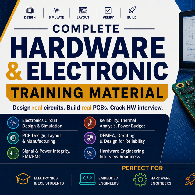
Complete Hardware and Electronic Training Material

Company Test Papers Electronics and Semiconductor
About me
Frequently asked questions
What is PCB design in electronics?
PCB design is the process of creating the schematic and physical layout of a Printed Circuit Board that mechanically supports and electrically connects electronic components. It covers component selection, placement, copper trace routing, and preparing manufacturable files. Nearly every electronic product — from medical devices and automotive systems to consumer gadgets — depends on a well-designed PCB, which is why skilled designers are always in demand.
How to design a PCB board?
The standard workflow is: define requirements, draw the schematic, select components, place them on the board, route the traces, run design-rule and signal-integrity checks, generate Gerber and drill files, and then prototype and test the board. Many beginners follow a structured PCB design tutorial before attempting their first board, because decisions like trace width, decoupling, and grounding directly decide whether the board works.
Which PCB design software should I learn first?
Free tools like KiCad are enough to learn the fundamentals of PCB design software workflows. If you are targeting industry jobs, exposure to Altium Designer or Cadence (Orcad/Allegro) helps, since many companies use them. Core concepts like schematic capture, layout, routing, and design rules transfer across tools, so master one first and adapt later.
How do I choose the right PCB design course?
Look for a PCB design course that includes hands-on projects on real boards, is taught by someone with actual industry hardware experience, and covers advanced topics like high-speed layout, signal and power integrity, DFM, and IPC standards — not just tool menus. Also check whether you get software access, project feedback, and end up with a portfolio you can show in interviews.
How do I prepare for a PCB design engineer interview?
Revise the fundamentals: schematic reading, layout guidelines, grounding and decoupling, signal integrity basics, stack-ups and materials, and IPC standards. Be ready to explain the trade-offs in your own projects in depth. Since many companies conduct written tests, practicing company-specific test papers for electronics and semiconductor roles along with mock interviews greatly improves your speed and confidence.
What are embedded systems in simple words?
An embedded system is a combination of hardware and software built around a microcontroller or processor that performs one dedicated task inside a larger device — for example, a washing machine controller, a car ECU, or a patient monitor. Unlike a general-purpose computer, it is optimized for a single function with strict limits on cost, power, size, and real-time response.
How to learn embedded systems from scratch?
Start with basic electronics and C programming, then move to a microcontroller platform and learn peripherals like GPIO, UART, I2C, SPI, ADC, and timers, followed by interrupts and RTOS basics. The fastest way to learn embedded systems is to build real projects — sensor interfacing, motor control, communication between boards — and read datasheets yourself instead of only watching lectures.
How to become an embedded systems engineer in India?
The usual path is an electronics-related degree, strong C programming and microcontroller skills, knowledge of RTOS and communication protocols, and a portfolio of hands-on hardware projects or internships. Then target automotive, defense, medical device, IoT, and semiconductor companies, and prepare specifically for their technical tests and interviews. Niche hardware skills like FPGA, hardware design, or firmware debugging help you stand out.
Is embedded systems a good career in India?
Yes. The growth of electric vehicles, defense and aerospace programs, medical devices, industrial automation, and semiconductor manufacturing in India is driving strong demand for engineers who understand both hardware and firmware. It suits people who enjoy working close to hardware, and salaries grow significantly as you build niche expertise, because experienced hardware talent is harder to find than software talent.
How do I choose an embedded systems course in Pune with placement?
Judge any embedded systems course in Pune with placement claims on four things: curriculum depth (C, microcontrollers, RTOS, protocols — not just demonstrations), lab hours on real hardware, live projects you can showcase, and the actual placement record with the companies that visit. Speak to alumni, compare fees against outcomes, and remember that a well-mentored program with project reviews beats a classroom with placement numbers but weak fundamentals.
What is the full form of FPGA?
The full form of FPGA is Field-Programmable Gate Array — a semiconductor chip whose digital logic can be programmed and reprogrammed after manufacturing using hardware description languages like Verilog or VHDL. Because the hardware behavior itself is configurable, FPGAs are widely used in defense, automotive, medical, and high-performance applications where custom, timing-critical logic is needed.
What is the FPGA design flow?
The typical FPGA design flow is: specification, RTL design in Verilog or VHDL, functional simulation and verification, synthesis, place and route, static timing analysis and timing closure, bitstream generation, and finally programming and validating the device on hardware. In professional projects, verification and timing closure usually consume the most effort, and the flow is iterated until all timing and functional requirements are met.
What is the FPGA design engineer salary in India?
The FPGA design engineer salary in India depends heavily on skills, experience, industry, and city. Freshers with strong RTL coding (Verilog/SystemVerilog/VHDL), verification, and board-level debugging skills typically start above average electronics fresher roles. Product companies in defense, automotive, and semiconductors generally pay better than service firms, and specialists in areas like high-speed design or FPGA-based systems command a significant premium with experience.
What is FPGA design for embedded systems?
FPGA design for embedded systems means using an FPGA as the processing or interface core inside an embedded product where custom parallel or timing-critical hardware is required — such as motor control, telematics, image processing, and high-speed data acquisition. FPGAs often work alongside microcontrollers, which handle sequential control logic. Learning it requires HDL skills plus an understanding of how the FPGA connects with memory, sensors, and processors on a real board.
How to design FPGA-based PCBs?
Designing FPGA-based PCBs requires careful power integrity (clean supply rails and proper decoupling), bank planning and I/O assignment, impedance-controlled high-speed routing for memory and configuration interfaces, solid grounding, configuration circuitry (JTAG/flash), and thermal management. Because FPGA devices have many fast-switching pins, stack-up design and simulation-aware layout must be planned from the start, and a structured bring-up sequence — power rails first, then configuration, then I/O — saves weeks of debugging.