Testimonials
Services


The Semiconductor Saga | For Students
Get a PhD Abroad
Semiconductor Consulting
The Semiconductor Saga | For Entrepreneurs
The Semiconductor Saga | For Semicon Professionals
The Semiconductor Saga | For Investors
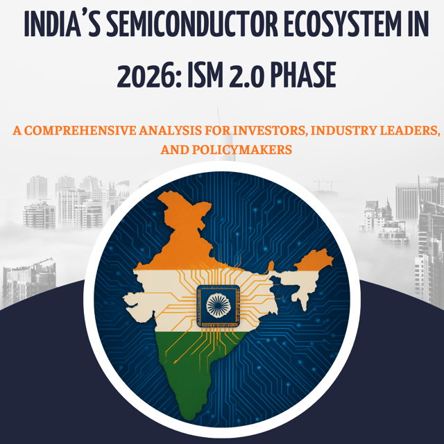
India’s Semiconductor Ecosystem in 2026 ISM 2.0
About me
- Kumar inspires and offers actionable insights, clarifying dilemmas with valuable suggestions.
 AI-generated based on testimonials
Frequently asked questions
What is the India Semiconductor Mission (ISM) and when was it launched?
The India Semiconductor Mission (ISM) is the Government of India's flagship programme, run under MeitY, to build a complete chip ecosystem in the country — semiconductor fabs, display factories, ATMP/OSAT packaging and test units, chip design incentives and talent development. The India Semiconductor Mission launch date was December 2021, with an initial outlay of ₹76,000 crore set aside to co-fund projects and support design-linked incentives for startups. Since then it has drawn multi-billion-dollar commitments, including India's first approved fabs and packaging plants.
What is India Semiconductor Mission 2.0?
India Semiconductor Mission 2.0 is the next, bigger phase of the government's chip programme, meant to scale up what India Semiconductor Mission 1.0 started between 2021 and 2025. While the first phase focused on seeding the country's first fabs, assembly-test plants and design incentives, ISM 2.0 pushes toward larger manufacturing capacity, advanced packaging, a stronger local supplier base and deeper design capabilities — the shift from "first plant approved" to a self-sustaining semiconductor ecosystem.
What is the India Semiconductor Mission 2.0 budget?
Unlike ISM 1.0, which was announced with a single ₹76,000 crore package, the ISM 2.0 budget is being committed project by project through MeitY approvals and successive Union Budget allocations rather than one headline number. Approved semiconductor projects under the mission already add up to well over ₹1.5 lakh crore in planned investment, so the practical way to track the second phase is to follow each fab, packaging and design approval as it is cleared.
Is India Semiconductor Mission 2.0 important for UPSC?
Yes. India Semiconductor Mission 2.0 for UPSC preparation is relevant across GS Paper III (economy, government schemes and science & technology), essays and the interview, because it ties together manufacturing policy, PLI-style incentives, chip-supply-chain geopolitics and India's digital economy. Aspirants should note the scheme structure, the major approved projects, and why semiconductor self-reliance matters for national security and economic growth.
How does semiconductor manufacturing work?
Semiconductor manufacturing works as a chain of specialised stages. A design company finalises the chip's circuit layout and hands it to a foundry, which builds the circuits layer by layer on silicon wafers inside a fab. The finished wafers are then cut into individual dies, packaged and rigorously tested — often by OSAT companies — before the chips go into phones, cars, data centres and industrial equipment. Front-end fabs and back-end packaging plants are usually separate facilities, and India is currently building strength in both to complete its domestic chip chain.
What is the semiconductor fabrication process?
The semiconductor fabrication process is the front-end stage of chipmaking, where transistors and interconnects are patterned onto a silicon wafer inside a fab. The wafer is cleaned and oxidised, coated with photosensitive resist, exposed through a photomask in a lithography scanner, etched to remove material, doped using ion implantation and polished flat with CMP — and this cycle repeats dozens of times to build up the layers. A single advanced chip can take months and hundreds of wafer-level operations, after which the back-end semiconductor manufacturing process steps of dicing, packaging and final test take over.
Where can I find a good semiconductor manufacturing process PDF, PPT, or flow chart?
Free semiconductor manufacturing process material is easiest to find in NPTEL and IIT lecture notes, university course pages, and government or industry explainer reports, while a quick image search gives ready-made flow charts and PPT slides. The limitation is that most free content covers only one slice — design, fabrication or packaging. If you want one continuous, India-focused walkthrough from raw silicon to a finished, packaged chip, a structured primer like The Semiconductor Saga book covers the entire manufacturing flow and the ecosystem around fabs and OSATs in simple language.
How does semiconductor packaging work?
Semiconductor packaging turns each die cut from a wafer into a protected, connectable chip. The die is mounted onto a substrate or lead frame (die attach), electrically connected through wire bonding or flip-chip bumps, encapsulated in moulding compound for mechanical and moisture protection, and then marked, singulated and re-tested before shipment. Advanced packaging adds wafer-level packaging, fan-out, 2.5D interposers and 3D die stacking — the technologies behind today's high-performance AI processors and a growing focus area for India's new assembly plants.
What is semiconductor packaging and testing?
Semiconductor packaging and testing are the back-end services that convert a finished wafer into qualified, shippable chips. Packaging gives the fragile die mechanical protection, power delivery, signal connections and heat dissipation, while testing screens out defective parts before they reach customers. Globally, this work is largely outsourced to OSAT (Outsourced Semiconductor Assembly and Test) specialists or handled in-house as ATMP, and this is exactly the segment India is now building out, with new assembly and test facilities coming up in Gujarat and Assam.
What is a semiconductor packaging substrate?
A semiconductor packaging substrate is the specialised layered board that sits between the silicon die and the main PCB. It fans out the chip's microscopic connections to a spacing the motherboard can handle, distributes power and helps remove heat, and is built from materials such as BT resin or ABF (Ajinomoto Build-up Film) with very fine copper wiring. Substrates are among the most critical and supply-constrained components in advanced packaging, produced by a small group of East Asian suppliers, which makes substrate manufacturing a strategic opportunity as India scales its packaging ecosystem.
What are the major semiconductor packaging companies in India?
The leading semiconductor packaging companies in India include Micron's ATMP plant in Sanand, Gujarat; Tata Electronics' assembly and test facility in Jagiroad, Assam; CG Power's OSAT unit in Sanand in partnership with Renesas; Kaynes Semicon's packaging plant; and SPEL Semiconductor, the country's long-standing OSAT player. More units are being approved under the India Semiconductor Mission, so this list is expected to keep growing as new plants come online.
Which semiconductor packaging course is best for beginners?
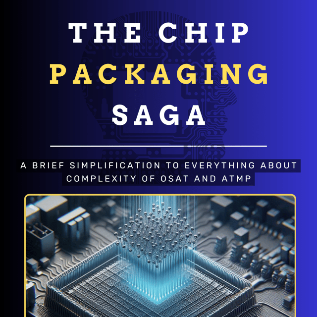
Pick a semiconductor packaging course that explains the whole back-end picture in plain language — assembly steps like die attach, wire bonding and flip-chip, substrates and materials, testing and reliability, and how OSAT and ATMP plants actually operate — rather than one that stays purely theoretical. Good entry points include NPTEL and IIT electives on microelectronics, MTech programmes in VLSI and microelectronics, and industry-oriented primers such as The Chip Packaging Saga, which is designed to make packaging and OSAT concepts clear for students and working engineers. Following news of India's new packaging plants also helps, since that is where fresher roles are opening up.
Is a career in the semiconductor industry a good choice in India?
Yes — a career in the semiconductor industry is currently one of the stronger engineering bets in India. It spans VLSI design and verification, embedded systems, fab process and integration, packaging, test and applications engineering, and demand is rising because India is adding fabs, packaging plants and global design centres at the same time. For ECE, EEE and VLSI students, the practical path is strong fundamentals, one clear specialisation, hands-on projects or internships, and staying close to industry developments — trained talent, not opportunities, is the real bottleneck in India right now.
How can Indian students secure a fully funded PhD abroad?
A fully funded PhD abroad for Indian students typically rests on three things: a research track record (a strong master's thesis, papers or projects), targeted outreach to professors whose work matches yours, and applications with funding built in through research/teaching assistantships and country scholarships. Shortlist a focused set of research groups, email professors with a specific, well-read pitch instead of a generic CV, and apply in the autumn cycle for the following year's intake. Kumar Priyadarshi followed this exact route — an IIT BS-MS, a published master's thesis at NUS, and six PhD offers from across the globe — so the process is very learnable with the right guidance.
What should I check before investing in semiconductor stocks in India?
Start with where a company sits in the value chain — design services, equipment and materials, packaging and test, or manufacturing — because the economics differ sharply: fabs need massive capital with long payback periods, while design and packaging services turn revenue faster. For semiconductor stocks in India, track participation in government incentive schemes, order books and capacity expansion, customer concentration, and the global chip demand cycle, since the industry is deeply cyclical and execution delays on new plants are the biggest risk. Reading an industry-oriented overview before buying helps separate long-term structural stories from short-term hype.